• Skip to primary navigation
  • Skip to main content
  • Skip to primary sidebar
  • Skip to footer

DisplayMonk

Solution to your problem

  • Home
    • Privacy Policy
  • About Us
  • Repair Tips
  • Schematics Bios
  • Course
  • Online Jobs
  • Tools
  • Enquiry / Contact
Home » Laptop Motherboard Repair

Laptop Motherboard Repair

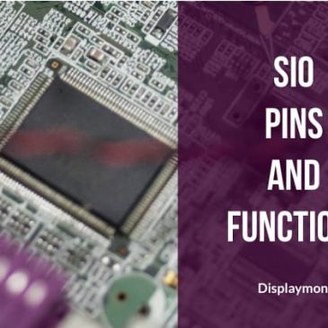
SIO Pins And Functions

May 4, 2022 by displaymonk

sio pins and functions


Firstly, before going to see SIO pins and their functions we will know what exactly is SIO. We will see it in this laptop motherboard repair guide.

SIO stands for Super Input Output Controller. SIO is sometimes called KBC or EC also. The Super I/O chip is managed in the motherboard it controls. also, it manages most of the I/O functions on the motherboard. Normally SIO has 128 pins.

Some Features Of SIO

Below are some features of sio

  • Control power and all switches
  • It manages fan and temperature
  • Manages keyword and mouse


Some Of The Common Manufacturers Of SIO

Below are some of the common manufacturers of SIO

  • ITE
  • SMSC
  • NUVOTEN
  • WINBOND
  • ENE


Signals To Run SIO

SIO requires four things to work. Below are signals to run SIO

Signal Work
VCC Gives the power to work 3.3 volt
EC_RTC EC RST means reset to SIO 3 volt
CLOCK 32.7 khz frequency from the main crystal
BIOS Bios input to execute commands


SIO Pins And Their Functions

Below are SIO pins and their functions


SIGNAL NAME TYPE DEFINITION
FRAME PCH to SIO frame signal from PCH indicating data processing
CLK 33mhz PCH to SIO 33mhz clock signal INPUT. It means the clock department is ok.
PLTRST PCH to SIO platform reset 3 volt saying all power ok reset generated.
BIOS_RD SIO to BIOS SIO reads BIOS
BIOS_CS SIO to BIOS SIO selects BIOS
BIOS_CLK SIO to BIOS clock signal
BIOS_WR SIO to BIOS write signal to bios
ACIN VIN to SIO adapter present signal
AC_PRESENT SIO to PCH adapter present signal to PCH
S5_ON SIO to Always always voltage turn on
SUSPON SIO to SUSPEND release always voltage to suspend
MAINON SIO to Step 2 turn on 1.5 volt, 1.05 volt
RUNON SIO to Step 2 turn on 1.5 volt, 1.05 volt
VR_ON SIO to VRM turn on CPU core voltage
SPS_PWROK PWM to SIO suspend voltage ok
HWPG PWM to SIO power ok to SIO without CPU
ECPWROK (PM_PWROK)SIO to PCH SIO to PCH  all power ok
TEMP_BAT BAT to SIO battery temperature
XCLK CLOCK 32.7 khz 32.7 khz input
RSMRST SIO to PCH resume and reset signal 3 volt
ECON SIO to PWM turn on 3.3 volt and 5 volt
PCH PWR ON SIO to MOSFET turn on PCH power
LAN_PWR SIO to LAN section turn on network
NBSWON (KBC_PWRBTN) PWR BTN to SIO power button 3 volt to zero
DNBSWON (PM_PWRBTN) SIO to PCH power on signal to PCH
SUSB (SLP_S3) PCH to SIO turn on power
SUSC (SLP_S4) PCH to SIO turn on power
USBPW_ON SIO to USB turn on USB
TPCLK SIO to TouchPad touchpad
TPDATA SIO to touchpad touchpad
MUTE SIO to Audio mute audio
FANSIG FAN to SIO fan rpm input to SIO
VFAN SIO to Fan turn on fan
PROHOT CPU to SIO CPU hot signal
SMBUS CLK SM BUS CLOCK system management signal
SMBUS DATA SM BUS DATA system management signal
KS SIGNAL KEYBOARD keyboard
ECRST reset signal to SIO
WIFI_ENABLE SIO to WIFI turn on the wifi card
LID_CLOSE LID SWITCH TO SIO LID SWITCH (magnetic sensor)
IMVP_PWRGD CORE TO SIO VRM CPU core voltage ok power good


Below Mention SIO Are Programmable

In the newer generation motherboard, EC BIOS merge into SIO means if SIO is bad then we have to replace SIO and copy EC BIOS into SIO. This SIO is called programmable SIO.

Below are some examples of programmable SIO’s:

  • ite it8585e programmable
  • ite it8586e programmable
  • ite it8985e programmable
  • ite it8587e programmable
  • ite it8522 programmable
  • ite it8587e programmable
  • ite it8589 programmable
  • ite it8522 programmable
  • ite it8380e programmable 192kb
  • ite it8586vg programmable
  • ite it8995e-128 programmable
  • ite it8886e programmable
  • ite it8386 programmable
  • ene kb9012 programmable
  • ene kb9016 programmable
  • ene kb9018 programmable
  • ene kb9022 programmable
  • ene kb9028qc programmable
  • ene kb9010 programmable
  • ene kb3930qf/b1 programmable
  • nuvoton npce288na0dx programmable
  • nuvoton npce388na0dx programmable
  • SMSC MEC 1609 programmable


In this way, you can do laptop motherboard repair using SIO diagnosing.


Thank you for your visit!!!!

Filed Under: laptop desktop chip level repair help guide Tagged With: Laptop Motherboard Repair, laptop motherboard repair guide, SIO Pins And Their Functions

Repair Laptop VRM Section – DisplayMonk

April 28, 2022 by displaymonk

Repair Laptop VRM Section

For doing repair the laptop VRM section we firstly must know that the laptop CPU VRM section generates CPU core voltage to the CPU. When all rest of the other power is ok then only CPU CORE voltage is generated. VRM chip work on 5 Volt and it requires enable signal to work called VR ON signal.

VRM chip first checks whether the laptop CPU is present from its VSENSE pin and the temperature from the NTC pin. Secondly, if everything is fine then the VRM chip starts triggering the MOSFETs, and CPU core voltage generates 1 Volt to 1.5 Volt and approx 30 Ampere current.

When the core voltage gets stable VRM chip generates IMVP PWRGD or VRM PWRGD signal. Moreover, the meaning of this signal is that CPU CORE power is ok and running.

List Of Signals And Their Descriptions For Laptop CPU VRM Section

The following is the list of signals and their descriptions for the laptop CPU VRM section :

SIGNAL NAME DESCRIPTION
VR ON VRM Chip gets this input signal to turn on core voltage.
VCC (VDD) 5 Volt power to VRM chip
VIN Volt input to VRM buck MOSFET
VCORE CPU CORE volt approx 1 Volt CORE volt consider in current
GFX CORE Graphics core voltage
VGATE VRM PWRGD When CPU core voltage is stable VRM chip sends out this power good signal
SVID CPU communicates with the VRM chip
VR HOT When the CPU portion gets very hot then the VRM chip sends out VR HOT low signal

Steps To Repair Laptop VRM Section

Below are the steps to repair the laptop VRM section

Check CPU Core

Firstly, Check whether the CPU core voltage for VCC pin is coming or not.

Check VR ON signal

Secondly, check VR ON signal is coming or not. If it’s not coming then check all previous voltages and SIO signals. If VR ON signal coming then come to the next step.

Check 5 Volt VCC

Thirdly, Check whether 5 Volt VCC is coming or not. However, if it’s not coming then check why 5 Volt VCC is not coming.

Check Switching Mosfets In Laptop VRM Section

Fourthly, check All Switching Mosfets available for the VRM section.

Replace CPU For Checking

Finally, if everything else is not working then as a final step replace the CPU and check if the motherboard working.

You can also visit for new books for training.

Filed Under: laptop desktop chip level repair help guide Tagged With: Laptop Motherboard Repair, laptop motherboard repair guide, Repair Laptop VRM Section, teps To Repair Laptop VRM Section

Power Sequence Of Laptop Motherboard

April 27, 2022 by displaymonk

Laptop Motherboard Power On Signals eg. SLP_4 SLP_3 SYSON SUSP VR ON

Understanding the power sequence of laptop motherboards is very important. Firstly the power sequence is the exchange of voltages and signals between the motherboard chips.

Secondly, This happens before anything appears on the screen.

The power sequence is the phase in which the motherboard prepares itself to function. This phase consists of sending orders to different voltage generators from some ICs. Secondly, receiving confirmation makes sure the principal Integrated circuits of the motherboard are functional.

The power sequence should take place in a specific order. Secondly, if one signal or confirmation is not sent or received then this phase stops there and finally, nothing will work.

The power sequence is used to troubleshoot laptop motherboard problems by testing voltages because the absence of some voltages indicates problems with some ICs. Also in some schematics, the power sequence is described which makes troubleshooting easier.

Steps To Check Voltage And Signal Sequence For Laptop Motherboard Power On Stage

The steps are known as ladders for voltages and signals. These steps are given below.

ALWAYS VOLTAGE Checking

This voltage generates before the power on the button is pressed. 3Volt is given to SIO and EC BIOS.

After Pressing The POWER BUTTON

Once the power button presses SIO to inform PCH and turn buck converters one after another.

POWER ON VOLTAGES check

The voltage after power should be produced as given below :

  • 3.3 Volt
  • 5 Volt
  • 1.8 Volt
  • 1.5 Volt
  • 1.05 Volt
  • CPU CORE
  • 0.9 GFX Core

POWER GOOD Signal Check

PCH receives SYS PWR OK signal confirmation signal saying all power is ok.

RESET Signal Check

PCH generates a PLTRST signal to clear motherboard junk values and reset the motherboard.

CLOCK SIgnal Check

CLOCK starts generating different frequencies according to the requirement of chips.

Starts Reading BIOS

In this step, the CPU starts reading BIOS.

POST Checking By Motherboard

In this step motherboard test all chips and devices in this process which is also called ‘Power on self test.’

Motherboard power states for understanding laptop motherboard power on sequence stages

These are the states of the laptop depending on the power consumption of the motherboard, you already know the two states which are :

  1. You turn on the Laptop.
  2. The laptop gets turned off by you.

The motherboard states are referred to in character ‘S…’ Where the x is a number between 0 and 5.

S0 State Of Laptop Motherboard

Working, the system is fully usable, all the components have their voltage.

S1, S2, S3 State Of Laptop Motherboard

Sleep, The laptop appears to be off, the laptop consumes less power than in S0 state, the RAM has its voltage, and is kept refreshed.

To wake the laptop from this Sleep state you need only to press a key on the keyboard or move the mouse.

S4 State Of Laptop Motherboard

Hibernate, the system appears to be off, and the power consumption is reduced to the lowest level. An image of the RAM is kept on the disc because RAM loses its voltages, to wake the laptop you need to press the power button.

S5 State Of Laptop Motherboard

In this step, the laptop motherboard gets shut down.

Types Of Motherboard Voltages For Power On Sequence Stages

There are four stages in the laptop motherboard which are given below:

Always Supply Voltage Type (ALWS or AUX or AL)

These voltages are always present even when the laptop is off, on one condition: the battery should be placed or the charger plugged in. Thises voltages are:

  • 5 Volt DC
  • 3.3 Volt DC

The 5 Volt and 3.3 Volt come from Voltage generator ICs in the motherboard.

Suspension Voltage Type (SUS ON)

These voltages are present in suspended or sleep mode (S1, S2, S3):

  • 5 Volt DC
  • 3.3 Volt DC
  • RAM voltage (For DDR1 – 2.5 Volt, For DDR2 – 1.8 Volt, For DDR3 – 1.5 Volt, For DDR4 – 1.2 Volt)

Note that the 5 Volt and 3.3 Volt are not the same % Volt and 3.3 Volt is Always voltage, there is another voltage generator that generates those 5 volts and 3.3 Volt.

Power On Voltage Type (RUN) (S0 State)

All the components have now their voltages. There is a supply of 1.05 Volt and 1.8 Volt is also done.

CPU Core Voltage Type

CPU requires core voltage, for example, a high current of approximately 20 Amp to 30 Amp. The newer motherboard graphics chip is also integrated into the CPU. So the graphics Core voltage is also required. These voltages are GFX core voltages. These voltages are approximate:

CPU Core = 0.8 Volt to 1.5 Volt / 20 Ampere to 30 Ampere.

GFX Core = 0.8 Volt to 1.5 Volt / 10 Ampere to 20 Ampere.

Laptop Motherboard Power Plane

There are two power input sources in a laptop motherboard one is adapter input and another is battery input.

The adapter input and battery charging section are called VIN ( Voltage Injection) sections. This section decides which power needs to be sent inside. This section has another task called battery charging. there are a number of buck convertors used according to fulfill the requirement.

Laptop Mother Powe Plane To Understanding Laptop Motherboard Power On Sequence Stages

Voltages Voltage Type
3.3 Volt Comes As Always Voltage
5 Volt This Also Always Voltage
3.3 Volt Suspended Voltage
5 Volt This Also Suspended Voltage
1.5 Volt System Run Voltage
1.8 Volt This Also System Run Voltage
1.05 Volt System Run Voltage
0.75 Volt This is Also a System Run Voltage
GFX Core Graphics Core Voltage
CPU Core CPU Core Voltage

Knowing the motherboard model number is important to find the laptop motherboard power sequence. Especially when we try to find out the Laptop Motherboard Power Sequences.

It helps to find pictures, schematics, board views, and known issues. There is always a number written on the board itself. In some cases, there’s also a sticker that tells a variant.

Common Laptop Motherboard Manufacturers For Laptop Motherboard Power On Signals

Below are some of the common laptop motherboard manufacturers

Quanta

Quanta motherboard found is HP, Dell, Acer, Toshiba, and a few Lenovo laptops. The model number on the board is “DA0xxxxMByyy” (first 0 is optional), “xxxxx” is the actual model, and “yyy” contains the revision. For example DAY11AMB6E0 for Quanta Y11A rev E.

Compal

Compal motherboard found in HP, Dell, Acer, Toshiba, Lenovo. Secondly, the model number is “LA-xxxxP” (P is optional), the older, the lower the number is like LA-4082P from 2007 or LA-E541P.

LCFC

Found in Lenovo, it’s actually Compal. The model number is “NM-xxxx”.

Wistron

Found in Acer, Dell, HP, Lenovo. The model number is an “xxxx-x” (x being a digit), often associated with a name. For example “Ricjie MB 11241-1”.

Inventec

They make Toshiba, HP, and Some Acer motherboards. Secondly, their model is number is often “xxyyzz” with “x”  being a letter, “y” a digit, and “z” as the optional letter.

There is also a “6050xxxxxxxx-MB-xx” number that can be easier to spot. For example “SA10E” and “6050A2052401-MB-A04” for Inventec.

Foxconn

Foxconn motherboards are found in Sony, Some HP laptops. HP has a weird model number like “CHICAGO_HR_HPCMV_MB_V1” or “PM_I_HPC_S_MV_MB_V3”.

Sony comes with an “MBX-xxxx” number that’s easy to identify, and other numbers, like “MBX-202” and “M790”.

Pegatron

Pegatron motherboards are found in a few Acer and Toshiba motherboards. Acer, in general, has an “xxyyzz” with “x” being a letter, “y” a digit, and “z” an optional letter. Toshiba has a weird model number like “PLF/PLR/CSF/CSRUMA”.

Whereas the following manufacturers make their own boards (except maybe a few models here and there):

Apple

Apple board model number is “820-xxxxx”, like “820-3462”. It’s written black on a black surface so it’s hard to spot.

Asus

Asus board model number follows the same format as the laptop model number. Secondly, It can be the same or similar, and sometimes different.

MSI

MSI model number is “MS-xxyxz”, with x being digits, y a digit or letter, and z an optional digit for revision. Some boards have two different model numbers like “MS-16J5” and “MS-1795” (with a 1 appended for the revision.

Samsung

Samsung model number is the name associated with a “BA41-xxxxxx” number, like “Bremen-D” and “BA41-01197A”.

Clevo

Clevo manufactures laptops for a lot of “small local” brands. There are two model numbers on the board, “6-71-W25S0-D02” and “W251ESMB-D0”.

HanStar doesn’t Design motherboards so we did not put them on the list. But rather HanStar manufactures the PCB. “J MV-4” and “94-V0” do not board model numbers, they are generic markings about PCB characteristics.

List Of Laptop Motherboard Power On Signals

The following are laptop motherboard power on signals:

SIGNAL NAME DESCRIPTION
VCC 3 Volt power to SIO and BIOS
ECRST RESET to SIO
LID SWITCH
THERMTRIP
The lid sensor should work
The thermal trip should normal
Clock SIO 32.7khz clock from either PCH
EC BIOS EC BIOS should perfect
RTCRST RTC RESET and crystal 32khz should to PCH
VCCDSW3_3 Power to PCH
DPWROK Power OK Indication for the VccDSW3_3 voltage rail
PWRBTN (NBSON) Power switch 3 – 0 – 3 variation
RSMRST SIO generates 3 Volt at this pin
PM_PWRBTN (DNBSWON) Post power button to PCH 3 Volt variation.
SLP_4
SLP_3
PCH generates 3 Volts send to SIO giving confirmation to turn on the power
SYSON, SUSP, VR ON All buck converters turn on one by one


Signal Name And Description For Laptop Power On Signals

When power is connected either from the adapter or battery to the motherboard it passes from various stages.

Below mention a chart given signal name and their description.

SIGNAL NAME DESCRIPTION
VIN voltage Check the input voltage to this current sensing resistor
VIN VIN is 3 Volt and 5 Volt section input voltage to 3 Volt and 5 Volt chip
VREG3 3 Volt linear output from 3 Volt and 5 Volt section which is going to SIO
VCC SIO gets 3 Volt at its power input pin
ECRST EC reset signal 3 Volt reset to SIO
THERMTRIP THERMTRIP thermal signal
LID SW LID SW is a magnetic lid sensor
BIOS EC BIOS starts communicating with SIO
NBSWRON /PWRBTN The power switch when we press 3 Volt goes zero and then again comes to 3 Volt. Moreover, you can see their 3 Volt variation.
ECON SIO generates an ECON signal and turns on always section 3.3 Volt and 5 Volt buck converter output.
3.3 Volt ALW,
5 Volt ALW
3.3 Volt and 5 Volt Buck converter output voltage.
PCH_PWR EN SIO generates this signal and provides power to PCH
VCCDSW3.3 PCH power management section gets 3 Volt power
DPWROK This signal is confirmation to PCH power 3 Volt
RTCRST RTC reset signal 3 Volt
SUSCLK 32.7KHZ clock frequency to SIO
RSMRST SIO sends a 3 Volt signal to PCH to reset and resume called RSMRST
DNBWORON
PMBTN
SIO sends post power button signal to PCH 3 Volt to zero and back
SLP_S4 (SUSB) 3 Volt power plane wake up signal to PCH to reset and resume called RSMRST
SPL_S3 (SUSC) 3 Volt power plan wake up signal from PCH to SIO
SYSON,
SUSP,
VR ON
SIO turn on all buck converter one by one


Power On Sequence Diagram For Laptop Power On Signals

Below are the diagrams for laptop power on signals.

power on sequence diagram one

Laptop Power On Signals For General Motherboards

Below is the power on signals for general Motherboards.

SIGNAL NAME DESCRIPTION
CURRENT SENSING RESISTOR Check here 18 Volt. Secondly, if not coming then check 1st or 2nd MOSFET or battery charging chip
VIN DC Voltage input to always voltage chips at its VIN pin
VREG3 3 Volt linear output from the chip
VCC 3 Volt power to SIO and BIOS
ECRST 3 Volt reset signal to SIO
AC OK 3 Volt signal coming from battery charging chip indicating power coming from adapter.
  SIO start communicating with BIOS
NBSWRON The power switch goes zero and comes back to 3 Volt
S5_ENABLE After the power button is pressed SIO generates an S5_ENABLE signal to 3 Volt and turns on the 3 and 5 Volt section
VCCDSW3_3 This 3 Volt power turn on PCH
DPWROK Power ok to PCH 3 Volt
SUSCLK 32.7KHZ clock frequency coming from PCH to SIO
RSMRST Resume Reset Signal
DNBWRON
PM_PWRON
Post power button signal generate from SIO to PCH
SLP_3
SLP_4
Wake up signal generated by PCH send to SIO
SUS ON
SYSON
Buck converter on signal

Laptop Power On Signals For Quanta Motherboards

Below is the power on signals for Quanta Motherboards.

SIGNAL NAME DESCRIPTION
3.3 VAL 3 volt linear goes to SIO VCC pin
PWRBTN NBSWON power button
SLP_S5 when power press SIO sends SLP_S5 signal to enable 3 Volt and 5 Volt supply
5 Volt 5 Volt buck converter output
3.3 Volt 3.3 Volt buck converter output
RSMRST SIO sends 3 signal PCH
PM_PWRBTN post power button from SIO to PCH goes low and back high
SUSC, SLP_S4, _S3 wake up signal sent by PCH to SIO to turn on the laptop
SUS ON This signal release 3 Volt and 5 Volt
5 Volt SUS  
SYSON system on signal turn on the buck converter
1.5 Volt (DDR3)  
MAIN ON main on signal turn on 1.05 Volt and 1.8 Volt
1.05 Volt, 1.8 Volt 1.05 Volt and 1.8 Volt
HWPG when all power ok then the HWPG signal generates 3 Volt and is given to SIO
VR_ON once SIO receives the HWPG signal is generated a signal to the VRM section
VCC / GFX CORE CPU core and GFX core voltage generated and given to CPU
IMVP PWRGD when CPU core voltage stable VRM chip sends this power good signal
ECPWORKS (SYS PWR OK) When all powers is ok including CPU SIO generates this 3 Volt signal to PCH
DRAM PWRGD ram power ok signal
PLTRST  
CS READ PCH read BIOS


Laptop Power On Signals For Quanta 4th Generation Motherboards

Below is the power on signals for Quanta 4th generation Motherboards.

SIGNAL NAME DESCRIPTION
POWER power input from the adapter and battery charging section. This voltage is approximately the adapter input voltage.
3.3 VAL this is 3 Volt linear output from the Always Voltage Section. This power goes to the SIO VCC pin.
PWRBTN (NBSWON) this is the power button. It is normally 3 Volt when we press a power button it goes to 0 and comes back to 3.
SLP_S5 this signal is sent by SIO to turn on Always voltage after the power button is pressed.
5 Volt 5 Volt and 3 Volt are always voltage.
3.3 Volt TO PCH this voltage to going to CPU to turn on its power. It is called VCC DSW.
RSMRST This is a 3 Volt resume signal generated by SIO to resume further sequence.
PM_PWRBTN This is a post power button from SIO to CPU.
SUSN, SLP_S3 Wake up the signal from the CPU to turn on different Buck converters.
SUS ON Suspend voltage turn on.
5 Volt SUS This is the 5 Volt and 3 Volt suspend output.
1.35 Volt (DDR3) 1.35 Volt buck convertor turned on.
MAINON Turn on the main power from SIO to the buck converter.
1.05 Volt 1.05 Volt buck converter turn on.
HWPG All power good signal when all the buck converter is working then HWPG signal is generated.
VR_ON CPU core voltage turn ON signal.
VCC_CORE CPU core voltage.
IMVP_PWRGD CPU core voltage ok.
DGPU_PWR_EN Graphics core voltage power good. This gives enables the signal to a 1.5 Volt buck converter.
GFXCORE Graphics core voltage.
DGPU_VC_EN Graphics core voltage power good. This gives Enable signal to a 1.5 Volt buck converter.
1.5 Volt 1.5 Volt buck converter voltage output.
DGPU_PWROK Power ok signal to SIO.
EC_PWROK All the power plans are ok including the CPU core, SIO generates this signal, even to the CPU.
SYS_PWROK All system powers are working fine.
PLTRST Platform reset. CPU generates the platform reset to reset the entire motherboard after it receives the system power ok signal.
DRAM RST PIN NO 30 Reset signal to the RAM.

Laptop Power On Signals For Wistron Motherboards

Below is the power on signals for Wistron Motherboards.

SIGNAL NAME DESCRIPTION
VREG 3 Volt 3 volt linear output from always section going to SIO power
S5 ENABLE from SIO to always section buck converter enable pin
VCCDSW this is the power to PCH 3 Volt
RTC CLK RTC section generates 32.7khz clock frequency after RTCRST signal
RSMRST resume and reset 3 Volt signal generated by SIO to PCH
PM_PWRBTN post power button signal generate by SIO 3 Volt variation going to PCH
SLP_S4 SLP_S4 signal is wake up signal sent by PCH to SIO.
SLP_S3 SLP_S3 signal is wake up signal sent by PCH to SIO.
1.8 Volt 1.8 Volt buck convertor turn on.
RUNPWRK after generating 1.8 Volt this buck converter generates power good
1.05 Volt RUNPWROK power good signal goes to 1.05 Volt buck converter.
VTTPWRGD when 1.05 Volt out then it generates power good and it goes enable to 0.85 VTT enable.
0.85 Volt 0.85 Volt buck converter turns on.
IMVP_VR_ON CPU core enables signal.
VCORE CPU core voltage output.
SYS_PWROK IMVP PWRGD signal generates after CPU core voltage stable and this signal goes to PCH. This signal sends all power ok called SYS_PWROK
DRAMPWRGD RAM power ok.
CPUPWRGD CPU power ok.
PLTRST platform reset generated by PCH and reset entire motherboard.


Laptop Power On Signals For WISTRON 5th Generation Motherboards

Below is the power on signals for Wistron 5th generation Motherboards.

SIGNAL NAME DESCRIPTION
ACIN adapter voltage input
VREG 3 Volt 3 Volt linear output from always 3 Volt and chip
S5_EN SIO sends this signal to enable 3 Volt and 5 Volt section
3 Volt and 5 Volt ALW buck converter output
RSMRST SIO sends resume signal to CPU
ON OFF SWITCH power button
PM PWRBTN post power button from SIO to CPU
SLP_S3 CPU generates this signal to turn on all buck converters.
1.35 Volt DDR3 supply turns on.
1.05 Volt / 1.5 Volt 1.05 Volt and 1.5 Volt buck converter turns on.
RUNPWROK power good signal
H_VCCST_PWRGD all power good signal
CPU CORE CPU CORE voltage
IMVP_PWRGD CPU power good signal output from VRM section
DRAMRST reset signal to DDR
BIOS CPU reads BIOS

For making a career in laptop chip level repair you must have knowledge about basic Chip Level components too.

There is also a guide for desktop motherboard power sequence which is similar but much smaller compared to laptop motherboards.

Filed Under: laptop desktop chip level repair help guide Tagged With: 5 Volt, CPU CORE, cpu power, desktop motherboard power sequence pdf, indicated power, laptop motherboard not getting power, Laptop Motherboard Power Sequence, laptop motherboard power supply, Laptop Motherboard Repair, laptop motherboard repair guide, laptop motherboard signals, laptop motherboards supplier, laptop power, laptop power sequence in hindi, mains power, motherboard voltage, motherboards power, mothers power, powder plans, powder press, power manage, power sequence of laptop motherboard pdf, power sequencer, power switch, processor power, provider power, SLP_3, SLP_4, SUSP, SYSON, systems power, volt power, voltage power, VR ON

Step Down Section 3.3Volt 5Volt Always Section

April 26, 2022 by displaymonk

3.3Volt 5Volt Always Section

Step Down Section 3.3Volt & 5Volt Always Section is the second section in the laptop motherboard. This section receives adapter voltage and generates 3 volts to get power to SIO.
Secondly, this section is also called as Always Voltage section. It has a Buck converter of 3.3volt and 5volt and two linear regulators called VREG3 and VREG5. Finally, if this section fails the laptop can’t turn on.

3v5v section in laptop reparing

Signals And Their Descriptions For Step Down Section 3.3Volt 5Volt Always Section

The below are Signals And Their Descriptions For Step Down Section 3.3Volt 5Volt Always Section:

SIGNAL NAME DESCRIPTION
VIN Input supply to Chip and MOSFET.
VREG3(LDO3) Linear 3 Volt output.
VREG5(LDO5) Linear 5 Volt output..
UG And LG UG = Upper MOSFET triggering
LG = Lower MOSFET triggering.
3ON(EN)
5ON(EN)
Input to 3 Volt and 5 Volt enable signal.
3VALW
5VALW
3.3 Volt always input
5 Volt always voltage output.
PGOOD Power good confirmation signal power ok.

LDO 3 Volt and 5 Volt Section In Step Down Section 3.3Volt 5Volt Always Section

This is another type of 3 Volt and 5 Volt section. In this type of supply only one linear output that is 5 Volt called LDO5 output and two Buck Converters for 3.3 Volt and 5 Volt.

SIGNAL NAME DESCRIPTION
VIN Input power to chip coming from adapter.
LDOEN LDO enable.
LDO Linear 5 Volt output.
VCC 5 Volt input to the chip.
ON3,
ON5
Enable signal to the chip.
3.3 Volt,
5 Volt
3.3 Volt voltage output.
5 Volt voltage output.
PGOOD Power good signal output.

Diagnosing Steps For Step Down Section 3.3Volt 5Volt Always Section.

Below are the steps for diagnosing step down 3.3 Volt and 5 Volt always section. Below is the flowchart for repairing 3.3 Volt and 5 Volt always sections in the laptop motherboard.

 Check 18 Volt Coming

Check for 18 Volt coming on VIN pin. moreover, it is depending on the laptop model which comes with a voltage between 18 to 21 Volt.

If it’s not coming then check why 18 Volt is not coming.

Check VREG = 3 Volt And VREG = 5 Volt Coming

Check if VREG =3 Volt And VREG = 5 Volt is coming n on the chip or not. If they are not coming then it means the chip may be bad or output circuit loading.

Check For 3 Volt ENABLE Signal

Check if the 3 Volt ENABLE signal is coming on the chip or not. Secondly if not coming, then check for why not getting that 3 Volt Signal. You can do different types of testing on the motherboard for that purpose.

3.3 Volt and 5 Volt Signal Is Coming?

Check for 3.3 Volt and 5 Volt voltages coming on the output coil or not. If it’s not coming then it can mean Chip itself or driving MOSFETs for that Chip may be bad.

If everything follows till now the 3 Volt and 5 Volt sections must be working correctly now. RT8205A, RT8205B, and RT8205C are some of the chips used for laptop chip level reparing.  Different chips are available for the Desktop motherboards for their problems.

Single Chip Buck Converter In Step Down Section 3.3Volt 5Volt Always Section

Single chip buck convertor is very popularly used in next generation motherboards. In this chip both switching MOSFET and PWM chip combined together. There is one Linear regulated output for 3 Volt or 5 Volt, also one PWM regulated output.

3 Volt Always Voltage For Signal Chip Buck Converter

Below are signals and their descriptions for  3 Volt Always Voltage For Signal Chip Buck Converter :

SIGNAL NAME DESCRIPTION
VIN Input Voltage to Chip.
LDO Linear voltage output.
ENABLE Enable signal to PWM.
OUTPUT 5 Volt input to the chip.
PGOOD Power good signal.

5 Volt Always Voltage For Signal Chip Buck Converter

Below are signals and their descriptions for  5 Volt Always Voltage For Signal Chip Buck Converter :

SIGNAL NAME DESCRIPTION
VIN Input Voltage to Chip.
LDO Linear voltage output.
ENABLE Enable signal to PWM.
OUTPUT 5 Volt input to the chip.
PGOOD Power good signal.

You can also check for the basics of laptop repairing to increase your knowledge.

Filed Under: laptop desktop chip level repair help guide Tagged With: Laptop Motherboard Repair, laptop motherboard repair guide, Step Down Section

Repair Laptop Battery Charging Section

April 25, 2022 by displaymonk

Repair Laptop Battery Charging

Below are the steps to follow to repair the laptop battery charging section :

Steps
Firstly, Check AD_ID signal in HP or in Dell laptop
Secondly, Replace the battery and recheck
Thirdly, Check voltage at the positive terminal when the adapter is plug
Fourthly, Check CHGEN signal or SM bus signals on battery charging chip
Fifthly, Replace battery charging chip and recheck
Sixthly, Replace battery charging MOSFET and recheck

Signals For Laptop Battery Charging Section

Signal Name Description
VIN Voltage input
DC IN DC power to the chip
AC IN (AC Detect) This 3 Volt signal indicates adapter current is present
AC DRIVE The signal drive adapter MOSFET
AC OK This 3 Volt output signal goes to SIO to indicate adapter current present
SMD, SMC BUS SM bus is two wire communication protocol between chip to chip
CSSP, CSSN Current sensor pin
BATDRV In some laptops, this signal is there. This signal drives battery MOSFET when adapter voltage missing
BAT_PRES When the battery connects to the motherboard this signal enables the battery current to the output

Battery Connector In Repair Laptop Battery Charging Section

Battery connectors have normally six connections Positive, Negative, SM Bus for communication Thermistor for battery temperature checking, and battery enables signal.

Connection Description
Positive + positive output
Thermistor SIO checks the temperature of the battery
Clock SM BUS is 2 wire communication protocol between SIO and battery
Data Data pin
Switch When the battery connects motherboard it enables the output volt
Negative Negative or ground signal

You can make a career and learn a laptop repairing course from us. Secondly, check for Component’s Code And Abbreviation On A Laptop Motherboard which is very helpful for identification of components on the motherboard.

Filed Under: laptop desktop chip level repair help guide Tagged With: Laptop Motherboard Repair, laptop motherboard repair guide, Repair Laptop Battery Charging

PCI Port And KQCPET6 Debug Card

April 20, 2022 by displaymonk

PCI Express and Debug Card


Firstly the use of PCI Express port is to diagnose desktop motherboards. Secondly, PCI ports come in 4 sizes 1x, 2x, 3x, and 4x. We are going to see PCI Port and Debug Card in detail

Signal Names And Their Description For PCI Express Port

The following is the signal’s name and description for the PCI express port.

3VSB (3V Stand By Signal )

3volt standby signal which comes before the power on button. If 3 volt here means SIO got 3 volt standby voltage.

3Volt VCC

It is a 3 Volt VCC voltage that comes after power on the desktop motherboard.

12Volt

After powering on the desktop motherboard 12volt voltage comes.

RESET

When all voltages including the CPU core OK then PCH generates 3 volts. Secondly, this signal is also called PLTRST ( Platform Reset).

CLOCK

Here we get clock frequency means the clock section ok.

SM Bus

This is the two wire communication protocol called SMBUS.

PCIE WAKE

If this PCIE WAKE generates 3 volt signal. This signal means the device is ready.


KQCPET6 Debug Card

KQCPET6 debug card has the following parts:

Check Switch

2digit code check switch is present there.

5 Pin Connector

Also, there is a present EC Wire 5 min connector.

Extension Socket

An extension cable socket is present there. Moreover, it connects the master card with T-Card or MiniPCIe adapter card.

USB Power Connector

There is also a USB power connector present. Secondly, it is used to connect to USB for power when using LPC or MiniPCIE connections.

Code Display

Firstly, It is also called BIOS and Qiguan display. It is moreover Qiguan 2 digit open code display and BIOS code.


What is the meaning of Debug Card LED

Below are the signals for which meanings are given for debug card LED.


LED Light Signal Type Description
AUX3V 3 Volt VSB LED should be lighted on after SMPS gets power and this 3 volt is given to SIO and PCH which is called standby voltage.
12V SMPS 12 Volt SMPS 12 volt power
-12V SMPS -12 Volt SMPS -12 volt power
RST RESET This LED would glow for a fraction of a second and then turn off. This indicates all motherboard chips got proper power.
CLK Main Clock This LED lights ON when there is a Clock signal.
FRAME Frame period LED flashes when there is a cycling FRAME signal indicating BUS in process.
RUN Run Status of CPU As soon as the CPU works, this LED will be ON.
IRDY Device Ready PCI device is ready when this light is on.
RAM Memory Error LED will glow continuously indicating that RAM /  desktop motherboard memory module or power fault.
CPU CPU Error LED steady ON of CPU indicates that the CPU did not pass the self test.
DISP Video Card LED will glow continuously indicating that the Video card / integrated motherboard GPU self test failed.
HDD/PCH HDD/BRIDGE LED will glow continuously indicating that Hard Drive / Bridges (North or South) / SATA / USB modules self test failed.
STABLE Stanble System LED will glow continuously indicating that The computer is stable, no error.
UNSTABLE Unstable System Computer motherboard is not stable, with potential faults.


You can go for more details about how the working of desktop motherboard happens or you can also look for other laptop repairing tips and tricks for more different subject understanding.


Thank you for your visit!

Filed Under: laptop desktop chip level repair help guide Tagged With: KQCPET6 Debug Card, Laptop Motherboard Repair, laptop motherboard repair guide, PCI Port

  • Go to page 1
  • Go to page 2
  • Go to page 3
  • Interim pages omitted …
  • Go to page 5
  • Go to Next Page »

Primary Sidebar

Search On Website

Laptop Desktop Chip Level Help Guide

  • Windows 10 Restarts After Shutdown

    Windows 10 Restarts After Shutdown

    March 24, 2025

  • T.VST59.031 Firmware Software

    T.VST59.031 Firmware Software Download Latest

    March 18, 2025

  • Mobile and Tablet Repairing Institute Class in Ratnagiri, Maharastra

    Mobile and Tablet Repairing Institute Class in Ratnagiri, Maharastra

    December 14, 2024

  • Laptop and Computer Repairing Institute in Ratnagiri, Maharastra

    Laptop and Computer Repairing Institute Class in Ratnagiri, Maharastra

    December 14, 2024

  • pm-modi-lic-sakhi-yojana

    LIC’s Bima Sakhi Yojana 2025: How To Apply?

    December 12, 2024

Footer

Mobile Repair

We do mobile repairing.

Learn more about mobile repairing service.

Laptop Repair

We laptop repairing.

Learn more about laptop repairing service.

TV Repair

We do TV repairing.

Learn more about tv repairing service.

Copyright © 2025 · DisplayMonk

  • Home
  • About Us
  • Repair Tips
  • Schematics Bios
  • Course
  • Online Jobs
  • Tools
  • Enquiry / Contact