• Skip to primary navigation
  • Skip to main content
  • Skip to primary sidebar
  • Skip to footer

DisplayMonk

Solution to your problem

  • Home
    • Privacy Policy
  • About Us
  • Repair Tips
  • Schematics Bios
  • Course
  • Online Jobs
  • Tools
  • Enquiry / Contact
Home » laptop motherboard repair guide » Page 3

laptop motherboard repair guide

vinafix.com at displaymonk for Power Sequence

April 19, 2022 by displaymonk

The Power Sequence In The Desktop Motherboard

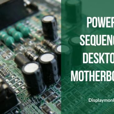
The power sequence in the desktop motherboard is the exchange of signals between the motherboard Chips that takes place before anything appears on the screen.

The power sequence is the phase in which the motherboard prepares itself to function. This phase consists of sending orders to different voltages and signal generators from some ICs and receiving confirmations. Secondly, It makes sure that the principal Chips of the desktop motherboard are functional.

The Power Sequence In The Desktop Motherboard Is Given Below

The following are steps for power sequence in a desktop motherboard :

1. Standby Voltage 5VSB

Standby Voltage 5 volt sent by SMPS from its purple wire and given to SIO VSB pin.

2 Power Button Press SMPS Turn On

When the power button is pressed then communication takes place between SIO and PCH and then SPMS tuns on. After it, all buck converters turn on one after another.

3. Power Good

Firstly Power Good is a confirmation signal given to PCH.

4. Reset

The reset signal clears any junk value that remains in the chips and all chips resume.

5. Clock

Clock chips provide different clock frequencies (timing) accordingly requirements of the chips.

6. BIOS

CPU read BIOS and run stat up sequence.

7. Post

In this step, BIOS checks power on self test.

8. DIsplay

When the motherboard completes all tests display appears.

The Signal Ladder For The Power Sequence In The Desktop Motherboard

The following are steps for the signal ladder for the power sequence in the desktop motherboard :

Step No Power And Signal Steps Description For Step
1 Stand Voltage 5VSB 5 Volt standby coming from SMPS going to SIO power on. Moreover, It is VSB pin before power on.
2 Power Button Press SMPS Turn On First up all voltages get Turn On. Secondly, power gets supplied to DDR, ICH, MCH, PCH, and CPU core voltages.
3 Power Good Confirmation signal from SMPS and VRM section saying all power ok.
4 Reset All power ok signals get generated after a successful Reset signal. Secondly, PCH generates a reset called FIRST. Lastly, This signal Clear’s motherboards all existed junk values.
5 Clock In this step, the Clock Chip or PCH generates different clock frequencies according to the requirement.
6 BIOS CPU reads BIOS
7 POST Power on self test does checkings for all chips.
8 Display In this step, the motherboard displays output on the screen.

The Signal Names And Description For The Power Sequence In The Desktop Motherboards

The following are signal names and descriptions for the power sequence in the desktop motherboards repair :

Signal Name Direction Description
VSB The purple wire from SMPS Standby voltage purple wire from the power supply.
RSMRST SIO to ICH (PCH) Resume and reset signal from SIO to ICH (PCH).
PSIN(PANSW) Power witch to SIO Power switch
PSOUT(PWRON) SIO to ICH (PCH) SIO asking permission to ICH (PCH) for power on.
SLP3(SUSB) ICH (PCH) to SIO Turn on power
SLP4(SUSC) ICH(PCH) to SIO Turn on power
PSON SIO to SMPS Turn on SMPS green wire 5 volt to zero volt
PLTRST ICH(PCH) Reset the entire motherboard platform reset
CLK_EN ICH to clock chip Clock enable
CPURST MCH to CPU Reset CPU 1 volt
CLK clock Clock signal
CPU_PWRGD ICH(PCH) to CPU CPU voltage ok
PWR OK SMPS to SIO Grey wire from SMPS
VCCORE VRM to CPU CPU core voltage
GFXCORE VRM to CPU(gfx) GRAPHICS supply ok
DRAMPWRGD PCH to CPU RAM power ok
CS PCH to BIOS Chip select signal PCH ready to read BIOS
VTT POWER To CPU Internal CPU voltages
VTT_POWERGD VTT power to CPU VTT power good or it means the VTT power section is in ‘ok’ condition.

When there is no display generated then you have to check all voltages including the CPU core.
Secondly, after the PLTRST signal is generated by ICH. Finally, CPU gets reset and the CPU access’s FSB bus.

The Power Sequence for New Generations Desktop Motherboards

The following are power sequences for new generations of desktop motherboards :

Number Signal Name Description
1 5VSB and 3VDUAL 5 volt coming from purple wire SMPS. This supply is then given to SIO.
2 DPWROK Power confirmation to PCH
3 RSMRST Resume and reset are then sent by SIO to PCH.
4 SIO to ICH (PCH) Power switch signal
5 PWRON In this power switch signal is sent by SIO to PCH
6 SLP_S4, SLP_S3 Wake up the signal sent by PCH to SIO
7 PSON Power on the signal sent by SIO to SMPS
8 H/W MONITOR SIO monitor signals
9 PWROK Power ok signal from SMPS to SIO
10 DDR_EN RAM power enables signal from SIO
11 VCC1_05_EN Enable signal from SIO
12 VCC18_EN Enable signal from SIO
13 VCC1_05_PCH 1.05 volt output
14 VTT_PWRGD VTT power good signal
15 VCORE CPU CORE voltage
16 VR_RDY CPU Core voltage ready signal
17 PWROK1 Power ok signal from SIO to PCH
18 PCH_VRMPWRGD CPU power ok signal
19 PFMRST When all power ok the PCH generates this signal called platform reset.
19 CPURST SIO generates CPU reset when it receives PFMRST

You can also see for laptop chip level repair career guide to kickstart your career.

Filed Under: laptop desktop chip level repair help guide Tagged With: Desktop Motherboard Repair, laptop motherboard repair guide, power sequence

Difference Between Intel Core i3 i5 and i7 Processors

April 13, 2022 by displaymonk

Difference Betwee Core i3 i5 and i7


The difference between i3, i5, and i7 is depending on various factors such as cores, caches, and threading. Firstly, we will go for checking for the main difference factors between Intel core i3 i5 and i7 Processors:

Cores Number

The more core there are in the CPU the more task can be served at the same time. This task is also known as Thread.

Turbo Boost

In Short, The Intel Turbo Boost Technology allows a processor to dynamically increase its clock speed whenever the need arises.

Cache size

Whenever the CPU finds that it keeps on using the same data over and over, it stores that data in the cache. The cache is just like RAM, only faster – because it’s built into the CPU itself. You can know more about the components of the CPU and the Identification of the CPU and its sockets.

Hyperthreading

Intel has introduced a technology called Hyper-Threading. This enables a single core to serve multiple threads.


What are the Changes In CPU By Intel Generation Wise

As generations of intel CPU chips grows there are absolute changes that have been made by the company. Below are changed by the company as the CPU upgraded :

  1. Introduced Nano Technology
  2. CPU core power also increased
  3. Number of cores increases
  4. Integration of graphics chip
  5. Integration of controller chip
  6. Cache memory increases
  7. Clock speed increases


What is the difference between Intel Core i3 i5 and i7 processors

i3 i5 i7
Cores 2 4 4
Threads 2 4 8
Turbo No 3.8ghz 4ghx
L3 cache 3MB 4MB 8MB


Difference between different generations of processors

Intel CPU Generations are code names for Intel CPU. They are given below.


Code Name Process Features Generations
Westmere (2010) 32nm 1st Generation CPU which is 20% faster than core 2 duo. Secondly, the memory controller is integrated into the CPU. 1st Generation
Sandy Bridge (2011) 32nm Integrated graphics and increased cache memory. Secondly, it is 10% faster than the 1st generation. 2nd Generation
Ivy Bridge (2012) 22nm Firstly, the basic difference is the DIE shrunk in size compared to Sandy Bridge. Moreover, it male improvement in graphics capability, and is targeted toward mobile applications. 3rd Generation
Haswell (2013) 22nm It has integrated PCH and a graphic chip. 4th Generation
Broadwell (2014) 14nm Firstly the basic difference is the DIE shrunk in size compared to Haswell to 14nm, which made an improvement in Thermal Design Power [TDP] 5th Generation
Skylake (2015) 14 nm This redesign gave better CPU and GPU performance. Secondly, It reduces power consumption. 6th Generation
Kaby Lake (2015) 14 nm Firstly, Kaby Lake is built on an improved 14nm process. Secondly, Kaby Lake features faster CPU clock speeds. Thirdly, the Clock speed get changes. Fourthly, Kaby Lake gets a higher Turbo frequency. Lastly, Kaby Lake is the first core architecture to support hyperthreading for the Pentium-branded desktop CPU SKU. 7th Generation
Coffee Lake 14 nm Coffee Lake has increased the core count. 8th Generation
Ice Lake 10 nm Ice Lake is firstly built on the Sunny Cove microarchitecture. Secondly, It has other features like :

  1. a 50% increase in the size of the L1 data cache,
  2. larger L2 cache,
  3. more microOP cache,
  4. increased 2nd level Thermal Design Power.
  5. Increased core width,
  6. Increment in execution ports (8 to 10),
  7. L1 store bandwidth doubled.
9th Generation
Comet Lake 10 nm Firstly, it consists of 10th Generation Intel Core processors. They deliver the following features:

  1. improved productivity and stunning entertainment,
  2. Including up to 5.3GHz,
  3. Intel Wiki 6,
  4. Thunderbolt 3 technology,
  5. 4K HDR,
  6. Intelligent System optimization.
10th Generation


You can also look for a laptop chip level repairing guide or desktop chip level repairing guide.


Thank you for your visit.

Filed Under: laptop desktop chip level repair help guide Tagged With: Desktop Motherboard Repair, Difference Between Intel Core i3 i5 and i7 Processors, Laptop Motherboard Repair, laptop motherboard repair guide

Components Of The CPU And Identification

April 12, 2022 by displaymonk

components of the CPU and identification

In the below sections, we are going to see the components of the CPU and identification.

A Central Processing Unit is a full form of CPU form. It is also called a central processor or main processor. also, It is the electronic circuitry within a computer that executes instructions that make up a computer program.

Secondly, The CPU performs basic arithmetic, logic, controlling, and input/output (I/O) op[erations specified by the instructions.

Registers

Registers are small holding areas of the processor chip. Secondly, Register holds data such as

  1. Counters,
  2. Data,
  3. Instructions,
  4. Addresses ALU (Arithmetic and Logical Unit).

Processor internal memory caches (L1, L2, L3)

Processor internal memory caches hold data and instructions also, ALU processes these instructions and data.

Busses

Basically, Busses are a component in the CPU that carries data and instructions. There are 3 kinds of buses in CPU:

  1. Front Side Bus (FSB)
  2. Internal Bus
  3. Back Side Bus

Processor Frequency (Speed)

Processor frequencies are the speed at which a processor operates internally.


What CPU Needs To Work

CPU needs the following 5 things to work:

voltages

There are voltages like DDR power, VTT power (system), CORE voltage & GFX voltages are used.

Power Good

Power Good is confirming the signal to inform the CPU that all power is stable.

RESET

RESET is a signal which clears all junk information.

CLOCK

The clock is a timing signal in form of frequency.

DMI

Firstly, the DMI bus gets activated after the CPU receives all the above signals. Then DMI bus access PCH.

You can also check for other kinds of checks that need to motherboard run.


Identification Of Intel CPU

A sSpec number is a specification number. It’s a fixed character string printed on the processor and used for identification. Secondly, By looking at the markings on the processor you can find the sSpec number. Moreover, SL36W and XL2XL are some of the examples of sSpec numbers.

You can also check how to identify components in the laptop motherboard which will be useful when you open the motherboard of the laptop/desktop for finding the CPU.


CPU Types And Sockets

Motherboards are subcategorized by the type of processor socket they have. Secondly, The processor socket (also called a CPU socket) is the connector on the motherboard that houses a CPU and forms the electrical interface and contact with the CPU. Finally, There is their type of CPU sockets are given below:

1. PGA :

In this PGA-type processor, sockets use a pin grid array (PGA). Secondly, we say their socket is PGA where pins on the outside of the processor are connected to holders in the processor socket.

2. LGA :

Land Grid Array (LGA) is a type of surface-mount packaging for CHIPS that is notable for having the pins on the socket (when the socket is used) rather than the integrated circuit. An LGA can be electrically connected to a printed circuit board (PCB) either by the use of a socket or by soldering directly to the board.

3. BGA :

Ball grid array (BGA) is a type of surface-mount packaging ( a chip carrier) used for integrated circuits. Second, BGA packages are used to permanently mount devices such as processors.


CPU Generations And Sockets

CPU generations get change according to the years they were manufactured. So there are given below CPU sockets and their generation Intel code names and supported PCH.

1. LGA 775 :

LGA 775 is a dual-core, core 2 due or quad-core CPU. It is used in

  1. G31,
  2. G41 motherboard.

2. LGA 1156 :

LGA 1156 is the core 1st generation CPU. Secondly, It is also called Westmere or Clarkdale. It is used in

  1. H55,
  2. P55,
  3. H57,
  4. Q57 motherboards.

3. LGA 1155 :

LGA 1156 is the 2nd and 3rd generation CPU. Secondly, It is also known as Sandy Bridge or Ivy Bridge. It is used in

  1. H61,
  2. H67,
  3. P67,
  4. Z68,
  5. B75,
  6. Q75,
  7. Z75,
  8. H77,
  9. Q77,
  10. Z77 motherboards.

4. LGA 1150

LGA 1150 is the 4th and 5th generation CPU. It is also known as Haswell or Broadwell. It is used in

  1. H81,
  2. B85,
  3. Q85,
  4. H87,
  5. Z87,
  6. Z97,
  7. H97 motherboards.

5. LGA 1151

LGA 1151 is used for 6th generation up to 9th generation CPU.

6th generation Skylake CPU uses :

  1. H110,
  2. B150,
  3. Q150,
  4. H170, and
  5. Z170 motherboards

7th generation Kaby Lake uses :

  1. B250,
  2. Q250,
  3. H270,
  4. Z270 motherboards.

8th generation Coffee Lake / Ice Lake CPU uses :

  1. H310,
  2. B365,
  3. B360,
  4. H370,
  5. C246,
  6. Q370,
  7. Z390 motherboards.


Types of sockets:

1. mPGA478MT (Socket M)

mPGA478MT socket uses intel core solo, intel core duo, intel dual-core Xeon, and intel core 2 duo processors.

2. mPGA478MN (Socket P)

mPGA478MN socket uses intel core 2 processors.

3. Socket 479

Socket 479 socket uses Intel Pentium M and Intel Celeron M processors.

4. Socket 478MB

Socket 478MB socket uses Celeron Pentium 4 Pentium 4-M processors.

5. Core I CPU Sockets

rPGA989, rPGA988A, rPGA988B are some of G1,G2,G3 generations sockets names.

So in this way, we learned about components of the CPU and identification.


Also can do  hot and cold testing which is part of doing laptop chip level repairing or desktop chip level repairing.


Thank you for your visit.


Filed Under: laptop desktop chip level repair help guide Tagged With: Components Of The CPU And Identification, CPU, Laptop Motherboard Repair, laptop motherboard repair guide

How To Repair A Dead Desktop

April 9, 2022 by displaymonk

Guide For Desktop Repair

In this section, we will get to have a guide for repair a dead desktop. how to repair a dead desktop? is one of the most asked questions asked by newcomers in the laptop/desktop repair industry.

There are different steps we can check for a guide to repair a dead desktop.

Step 1. Check #VSB Supply Coming On SIO for repairing motherboard

Firstly check whether the 3 VSB supply is getting reached to SIO. If it is not coming then check whether 5volt coming from SMPS purple wire. If not then check SMPS, or there is a possibility is that the 3volt regulator is bad.

Step 2. Check whether the RSMRST signal is coming on SIO for the dead motherboard

Secondly, if the 3VSB supply is coming on SIO Pin then check whether the RSMRST signal is coming on SIO. If it’s not coming then there is SIO of your computer is bad.

Step 3. RTC Clock On PCH on a desktop motherboard

In the third step for dead desktop repair checking and repair check for RTC clock signal is coming on SIO. If it is not coming then replace and check the 32.7khz crystal. IF even if the RTC clock signal is not coming then Replace PCH.

Step 4. Check RTCRST SIgnal

Check there the RTCRST signal is coming as the RTCRST signal is very important in desktop repairing check. RSMRST stands for ResumeReset Signal.

Step 5. SLP_S3 (SUSB) is coming on SIO

SLP_S3 stands for Sleep S3 signal. It is important to signal for the desktop to work. Check where it is coming from on the SIO pin. If it is not coming check the DPWROK signal to PCH. Then, If it is coming then replace PCH. Finally, If it’s not coming then replace SIO.

Step 6. PSON Signal Going To SMPS on a desktop motherboard

Even if the SLP_S3 signal is coming properly and the desktop is not starting then check for the PSON signal. Check whether the PSON signal is going to SMPS. If it is not going to SPMS replace SIO.

Step 7. Replace SMPS

Finally, if nothing works from the previous steps then replace SMPS. This is the final step of repairing a dead desktop repairing.

Learning Further For Chip Level Repairing

There is a basic guide for desktop repairing guide and some schematics diagrams available which you can use to trace the current flow.

Also, you can do repairing for laptop motherboard for basic repair and advance /chip level repair.

thank you very much for your visit…

Filed Under: laptop desktop chip level repair help guide Tagged With: Desktop Motherboard Repair, Guide For Chip Level Repair Dead Desktop Motherboard, laptop motherboard repair guide

Regulated Power Supply In Motherboard

April 8, 2022 by displaymonk

Types Of Regulated Power Supply


Motherboard chips require normally 1.05volt, 1.5volt, 3.3volt, and 5-volt power supply. But, the Laptop Adapter Charger Repair gives 18 volts or 19 volts these volts to regulate. We can see them in the laptop chip level repair guide. Here we are going to see Regulated Power Supply In Motherboard. There are two types of regulated power supplies:

  1. Line regulator,
  2. Buck converter regulator


Linear Regulator Power Supply

Linear Regulator Power Supply Used In Motherboard

Linear component is used in a linear regulator to regulate the output. An example of a linear component is Resistive Load.


Buck Converter Power Supply

Buck Convertor In Regulated Power Suplly Used In Laptop Motherboard

A buck converter is a DC to DC power converter that steps down the voltage from its input to its output.

It is a class of switched-mode power supply typically containing at least two semiconductors and at least one energy storage element, a capacitor, coil, or the two in combination.

The circuit for the buck convertor operates by varying the amount of time in which the inductor receives energy from the source.

In the basic block diagram, the operation of the buck converter or buck regulator can be seen that the output voltage appearing across the load is sensed by the sense/error amplifier and an error voltage is generated that controls the switch.

Typically the switch is controlled by a pulse width modulator However, The switch remains longer as more current is drawn by the load.

Lastly, mostly there is a fixed frequency oscillator to drive the switching.


Typical Buck Converter

Below types of buck convertors are there in desktop and laptop motherboards.

In a buck converter, two MOSFETS use for switching voltages. One PWM chip uses to trigger these two MOSFET

alternatively.

Coil gets switching voltage as a load current. Capacitors use there to filter and store voltage.

That’s it guys, if you want to know about the basics of laptop repairing or brush up on them then you can check our basic guide for laptop repairing.


Finally, You can also check our other laptop preparing help guides.


thank you for your visit…


Filed Under: laptop desktop chip level repair help guide Tagged With: Laptop Motherboard Repair, laptop motherboard repair guide, types of power supply

Laptop Desktop Repairing Architecture Structure

April 7, 2022 by displaymonk

What Is Computer Architecture

Computer architecture is firstly made up of different components which we will give in online guide for structure of laptop for reparing.

When all the components are collectively represented then it’s called the entire computer architecture. Components present there has a variety like,

  1. CPU,
  2. NorthBridge,
  3. RAM,
  4. Hard Disk Drive,
  5. SouthBridge,
  6. BIOS,
  7. Super IO, etc.

In the following sections, we are going to see information about Computer architecture sections like:

  1. Bus Architecture,
  2. Form Factor,
  3. Chipset,
  4. Repair Flowchart,
  5. Schematic Diagram,

Computer Bus Architecture

Bus In Computer Architecture

In computer architecture, a bus is a communication system that transfers data between chips inside a motherboard, or between computers.

Secondly, This expression covers all related hardware components (wire, optical fiber, etc.) and software, including communication protocols.

Lastly, some common buses are FSB, DMI, SPI, LPC, etc.

Form Factor In Computer Architecture

form factor computer architecture

With the advancement in technology computer motherboard has been dramatically changed they differ in

  1. shape,
  2. size,
  3. compatibility,
  4. the capacity to hold the CPU.

There are many big companies which manufacture motherboards these days. They follow some common guidelines such as placement of CPU sockets, RAM slots, Expansion slots, USB, IDE, SATA Ports, and connectors.

These guidelines are called a Form Factor.

Role Of Chipset In Computer Architecture

Chipset In Laptop Motherboard

A chipset is a set of BGA chips known as a “Data Flow Management System”. Moreover, it manages the data flow between the CPU, RAM, BIOS, and peripherals. It is usually found on the motherboard.

Chipsets are usually designed to work with a specific family of processors.

Because it controls communication between the processor and external devices, the chipset plays a crucial role in determining system performance.

Secondly, The term chipset often refers to a specific pair of chips on the motherboard: the northbridge and the southbridge.

The northbridge links the CPU to very high-speed devices, especially RAM and graphics controllers, and the southbridge connects to lower-speed peripheral buses.

The southbridge contains some on-chip integrated peripherals, such as Ethernet, SATA, USB, and audio devices.

Newly, In some new generation motherboards, Intel merges the northbridge and southbridge other and makes a new chip called PCH which works both jobs.

Repair Flowchart

Repair Flowchart Computer Architecture

A flow chart is a combination of

  1. a common type of diagram, which represents an algorithm or process,
  2. showing the steps as boxes of various kinds,
  3. Order points 1 and 2 by connecting these with arrows.

Flowcharts are used in the career of laptop repairman to find out faults in laptop motherboard. To diagnose the motherboard you have to follow from top to bottom.

Schematic Diagram For Computer Architecture

Schematic Diagrams In Computer Architecture

When working with circuits, you will often find something called a schematic diagram.

These diagrams use symbols to illustrate electronic components in the circuit.

In conclusion, These symbols are graphic representations of the actual electronic components.

thank you for your visit…

Filed Under: laptop desktop chip level repair help guide Tagged With: Computer Architecture, Desktop Motherboard Repair, Laptop Motherboard Repair, laptop motherboard repair guide

  • « Go to Previous Page
  • Go to page 1
  • Go to page 2
  • Go to page 3
  • Go to page 4
  • Go to page 5
  • Go to Next Page »

Primary Sidebar

Search On Website

Laptop Desktop Chip Level Help Guide

  • Windows 10 Restarts After Shutdown

    Windows 10 Restarts After Shutdown

    March 24, 2025

  • T.VST59.031 Firmware Software

    T.VST59.031 Firmware Software Download Latest

    March 18, 2025

  • Mobile and Tablet Repairing Institute Class in Ratnagiri, Maharastra

    Mobile and Tablet Repairing Institute Class in Ratnagiri, Maharastra

    December 14, 2024

  • Laptop and Computer Repairing Institute in Ratnagiri, Maharastra

    Laptop and Computer Repairing Institute Class in Ratnagiri, Maharastra

    December 14, 2024

  • pm-modi-lic-sakhi-yojana

    LIC’s Bima Sakhi Yojana 2025: How To Apply?

    December 12, 2024

Footer

Mobile Repair

We do mobile repairing.

Learn more about mobile repairing service.

Laptop Repair

We laptop repairing.

Learn more about laptop repairing service.

TV Repair

We do TV repairing.

Learn more about tv repairing service.

Copyright © 2025 · DisplayMonk

  • Home
  • About Us
  • Repair Tips
  • Schematics Bios
  • Course
  • Online Jobs
  • Tools
  • Enquiry / Contact